- Home
- Assembly AND PARTS LIST
- PROJECTS
- BUY
- EMF, MONOSTABLE, COUNTER
- PIC BASIC EXAMPLE PROGRAM
- LOGIC GATE EXPERIMENT
- LDR AND VCO VIDEO
- LAB VIDEOS
- MORE
- ARDUINO
- CONNECTION TO WS2811 LEDS
- 24 BIT SHIFT REG CODE
- 24 BIT SHIFT REG CODE (2)
- USING SHIFT REGISTERS
- DRIVING A STEPPER MOTOR
- CASCADED DOT MATRIX DISP
- LED LABS SILK SCREEN
- SOME EXPLAINED SCHEMATICS
- LOGIC TRUTH TABLES
- LEDLABS VIDEO
- LED LAB & GOLDEN SPIRAL
- SIGNAL DEGRADATION
- TRANSISTOR OUTPUT TEST
- LOGIC GATES
- CHOOSING POTENTIOMETERS
- LOTTERY GENERATOR IDEA
PROJECTS

PROJECTS AND INFORMATION FOR THE NEW REVISION LAB AND EARLIER VERSION TO ARRIVE SOON
PICTURE OF EARLIER LED LAB

AN INTERESTING ARRANGEMENT THAT DISPLAYS SOME LIGHTING EFFECTS WHEN MUSIC IS PLAYED.
CONNECT THE MODULES AS SHOWN.
THE BREAKOUT PORT BECOMES THE OUTPUT OF THE PWM, DUE TO THE CONNECTION OF THE BUFFER, THIS ALSO ALLOWS MORE CONNECTIONS TO DRIVE MORE DEVICES. THE CARRY OUT OF MODULES CAN ALSO DRIVE INPUTS. NOTE THE 555 CLK OUT IS ATTACHED TO DATA IN OF SHIFT REG AND NOT CLOCK, IN THIS EXAMPLE. ALSO T

THIS DIAGRAM SHOWS WHAT THE LOAD DOES IF A HIGH INPUT OR LOGIC 1 IS PRESENTED TO THE INPUT OF THESE WIRING TRANSISTOR CONFIGURATIONS.
CONNECTION TO SWITCH DEBOUNCE
AND SPARE INVERTERS
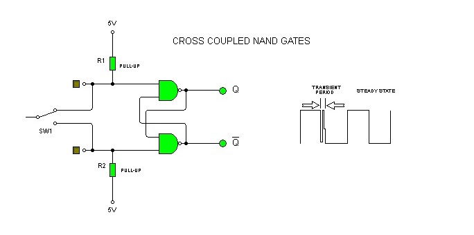
Switch debounce is a useful small delay in a circuit to minimize the mechanical oscillations after a switch has been pressed.
Due to these mechanical oscillations, a logic IC could read a secondary bounce or further bounces as a logic level and act on this signal further advancing the decision process of the IC,
consequently yielding incorrect outcomes.
Each type of switch has different bouncing characteristics or transient periods, until it reaches its steady state condition, and to eliminate this a switch debounce circuit is used in the form of maybe; two cross coupled nand gates the basis of a flip flop, RC delays or schmitt triggers.
Some switch debounce actions can be performed in software by simply adding a time delay to the code, say 10mS.
The nand gate configuration is a bistable (a basic memory device) stable in one state or the other and can hold one bit of information until toggled, a flip flop is said to flip from one state and flop to another.
Below shows a diagram of cross coupled nand gates as switch debounce configuration to eliminate the transient periods of mechanical switching, due to the sr latching action.
LedLabs has a rc time fed into a schmitt trigger hex inverter, and when a switch is pressed it makes the input to the schmitt trigger 0v, as it is an inverter a logic 1 is present at the output when this condition occurs.
Connect a free switch to the switch input, (not a pull up or pull down type) either on the lab or different type using both connectors of the switch, the circuitry is wired on the module, it grounds one of the switch contacts and connects the other to the appropriate components, the output can be connected to the 4026 counter clock in.
By way of example pressing the pulse button on the counter module which is not debounced a clean increment of the count is not always observed, the schmitt debounce gives a steady counter increment, it shows how switch debounce with the schmitt trigger cleans up the signal and passes it on to the logic device.
The image below shows a switch and input to the schmitt trigger debounce module whose output can connect to modules
The spare hex inverters are very useful to and are for free use, one example of use here is, inverting the binary ripple counter, to test this feed the clockout of a 555 timer into the ripple counter on around 1-2 hz so it can be seen, the lights of the 555 timer and the ripple counter look antiphase, this is because the ripple counter is falling edge triggered, feed the 555 clock in to a spare hex inverter input (the otherside of the switch debounce) then feed the output in to the ripple counter. and observe they are now in synchronisation and in phase as the hex inverter as inverted the signal.

WORKING OUT A SERIES RESISTOR FOR A GIVEN LED
To work out a series resistor for a given led, the equation is shown below
So if for example the supply voltage is 12v and the voltage drop of the led is 3v
and the led current is 20 ma maximum, this equation will allow a resistor of 450 ohms,
to make it shine at its brightest, this is however the minimum value for the resistor,
any value lower could damage the led, it's good practice to move the value up to say a 1k
in this example opposite to keep within the limits unless it is essential that maximum brightness
is needed. The information for a given led is found on data sheets for the device.
So a resistor in series with the led wired to the supply is the usual way to do this with the
anode wired to the + rail , the resistor can connect either to the cathode or anode of the led
, (cathode is denoted with a flat part on the led), and the anode usually has a longer leg.
Power ratings is also a consideration for larger current types of leds, as this would move
the power rating of the resistor up. If a 12v led was used and the supply was 12v,
generally no series resistor would be required, another way to use without resistors
, could be this way, if 4 x 3v leds were used with a 12v supply, the PN junctions of the diodes
would drop 3 volts each if wired in series, so 3v x the 4 leds equals 12v.
This is for low power types and not heavy duty types as a condition called thermal runaway
could occur with heavy current types, so the series resistor regulates and maintains the working conditions of the led


HERE IS THE FORMULA FOR CALCULATING THE SERIES RESISTOR (RS) FOR A TYPICAL LED.
THE RESISTOR VALUE CALCULATED IS THE SAFEST MINIMUM VALUE AND CONSEQUENTLY LIGHTS IT AT ITS BRIGHTEST. 1K AND UPWARDS IS FINE TO USE HERE AND WOULD START TO DIM THE LED FOR HIGHER RESISTOR VALUES.
THE LED CURRENT IS USUALLY DETERMINED BY THE DATA SHEET, IN THIS EXAMPLE IT WAS 20mA.

AN ELECTRIC FIELD DETECTOR WITH MASSIVE GAIN (hFE), USING A NPN SMALL SIGNAL TRANSISTOR WITH A GOOD GAIN OF SAY 100, WOULD CREATE 100X100X100 = 1000000 A GAIN OF A MILLION. TO USE AS A GHOST DETECTOR ADD THE HIGH PASS FILTER TO FILTER OUT LOW FREQUENCY LIKE THE 50-60HZ MAINS. THIS MASSIVE GAIN CAN BE NO LARGER THAN THE POWER SUPPLY, MICRO-VOLTS IN, SEVERAL VOLTS OUT.

DIAGRAM SHOWS BOTH PASSIVE AND ACTIVE, HIGH AND LOW PASS FILTERS.
Two circuit modules Arranged in a way containing a resistor and capacitor form the basis for an Integrator and a Differentiator, and depending on the waveform put in also act as low pass filter or a high pass filter. And the most basic type is a passive network arrangement containing these two components., drawing on the signal pro

HIGH PASS, LOW PASS FORMULA FOR CUT OFF FREQUENCY, WITH A ROLL OFF FREQUENCY OF 20dB/DECADE FOR A FIRST ORDER FILTER.
FOR EVERY FACTOR OF 10 FREQUENCY INCREASE THE FILTERS OUTPUT WILL DECREASE OR ATTENUATE BY 20dB.
SOME USEFUL FREQUENCY BANDS AND THEIR CORRESPONDING FREQUENCIES IN Hz.

UNITY GAIN AMPLIFIER GAIN = 1
OTHER NAMES VOLTAGE FOLLOWER
NON-INVERTING BUFFER..
THIS IS VERY USEFUL IN CIRCUIT COMPONENT LINKING AS IT HAS VERY HIGH INPUT IMPEDANCE AND LOW OUTPUT IMPEDANCE TO DRIVE THE NEXT CIRCUIT ELEMENT. WITHOUT THIS, IN SOME CIRCUITS IF THE LOAD IMPEDANCE OF A COMPONENT OR DEVICE IS LOWER THAN THE SOURCE IMPEDANCE THE OUTPUT VOLTAGE ETC WOULD DROP CONSIDERABLY.
AS A RULE O

INTERESTING SOUND EFFECTS FROM THE VOLTAGE CONTROLLED OSCILLATOR (VCO) USING THE LDR CIRCUITS AND/OR 555 TIMER AND THE LM386 AUDIO AMPLIFIER.
A VIDEO OF THIS PROJECT IS LISTED UNDER MORE IN THE DROP DOWN MENU.

EXPERIMENTS WITH LOGIC GATES USING SINK AND SOURCE, THE SAME FOR MICRO PIN OUTPUTS

A BASIC MICROPHONE BIASING CIRCUIT WITH A SMALL GAIN AND PWM OUT.
ALTERNATIVE MIC BIASING CIRCUIT

METRONOME CIRCUIT USING A 555 TIMER AND LM386 AUDIO AMPLIFIER
An easy way to build a metronome, which are used by some musicians to keep in beat, and these produce a series of ticks at regular time intervals or beats per minute, a 555 timer circuit in astable mode can be used, with a varying frequency, like the one on LedLabs board, all that requires adding to the clock output (pin3) is an electro

WIRING DIAGRAM FOR LEDLABS ON BOARD VOLTAGE CONTROLLED OSCILLATOR, PIN 1,2 NOW OMMITED.

SINK AND SOURCE 555 TIMER

PIN ASSIGNMENT FOR SEVEN SEGMENT DISPLAY

CIRCUIT DIAGRAM OF THE 555 ASTABLE INTEGRATED INTO LED LABS

CIRCUIT DIAGRAM OF THE 555 MONOSTABLE INTEGRATED INTO LED LABS

LED LABS 4026B COUNTER, THE CARRY OUT FUNCTION CAN BE CONNECTED TO THE NEXT DISPLAY

LED LABS PULL-UP SECTION, BUTTON COMMAND AND OTHER WIRING DIAGRAMS

LED LABS LM393 COMPARATOR SECTION.

LED LABS THERMISTOR AND LIGHT DEPENDENT RESISTOR SECTION.

LED LABS LM3914 WIRING SECTION
THE LM3914 SECTION CAN BE CHANGED TO A VU METER TYPE LM3915, OR LM3916, AS THE PINOUTS ARE THE SAME.
ANY PROBLEM WITH SWITCHING IN DOT MODE, THAT IS TO SAY LEDS 9,10, THAT LED 9 DOES NOT SWITCH OFF WHEN LED 10 TURNS ON.
THE 2.2K OR 1.2K RESISTOR, SOME LABS HAVE A 2.2K FITTED HERE, A 1K SOLDERED TO THE BACK OF THE PCB ACROSS (IN PARALLEL) WITH THE 2.2K
CURES THIS NIGGLE

LED LABS LARGE LED SECTION

LED LABS STEPPER MOTOR WIRING DIAGRAM.

ACTIVE OP-AMP CIRCUIT

10 SECOND TIME DELAY, VOLTAGE FOLLOWER CIRCUIT AND ITS EXPONENTIAL DECAY THE SMALL VOLTAGE DROP OF THE DIODE .7V ENSURES THE LED TURNS OFF.
THE RC TIME CONSTANT IS T= R*C IN SECONDS. AND IS SAID TO BE FULLY DISCHARGED AFTER 5 TIME CONSTANTS. PRESSING THE SWITCH BRINGS THE CAPACITOR CLOSE TO THE POWER SUPPLY VOLTAGE WHOSE OUTPUT THEN FOLLOWS THE INPUT, REPRESENTED BY A VISUAL LIGHT. WITHOUT THIS BU

A BASS FILTER WITH R1 AND C1 FORMING THE LOW PASS FILTER WITH A GAIN OF 10 FROM THE FIRST OP-AMP WHOS OUTPUT IS FED INTO ANOTHER OP-AMP CONFIGURED AS A COMPARATOR. NO DC FILTER CAPACITOR IS PRESENT BETWEEN THE OP-AMPS AND WOULD SIT AROUND 2 VOLTS ABOVE GROUND.
THE POTENTIOMETER OR VREF CAN BE SET AROUND THIS VOLTAGE SWINGING ABOVE OR BELOW.
THE PWM OUT IS 0V OR 5V, AND ITS MARK SPACE RATIO IS DETE
CHARGE/DISCHARGE OF CAPACITOR ON VU-METER
An easy way to see the charging/discharging of a capacitor through a resistor is to select a value for T, in the equation T = R*C.
The above values work out to be 10 seconds as 100000R x .0001uF = 10. Wire a resistor and a capacitor on the breadboard as shown above, and connect a wire from where they meet to the input of the Lm3914, (high input impedance so will not load the RC network) the power is just connecting to 0v and 5 volts on ledlabs, allowing the 5v to connect when you want the timing to start.
A rising voltage is seen on the lm3914 as the capacitor charges and after 10 seconds (1T) it has reached 63 percent of 5v, which may lay around just over half way on the lm3914 (3.15v) as this scale is 0v-3.6v., after the first time constant, a rate of change can be noticed on the leds output of the lm3914 with respect to time, this is, it is taking longer for the remaining leds to light, ie the growth of amplitude or voltage is not getting much higher within the same time frames(remember (5T) is beyond the 3.6v scale of the lm3914, so the capacitor goes on charging. Disconnecting the 5v rail shows the exponential decay of the capacitor through the leds on the lm3914.

experiments with audio
From a music source, ie a laptops headphone output socket, the small signal output can be amplified and connected to the audio amp on LedLabs and then fed to the 8 ohm speaker, one way to do this is to use a 3.55mm stereo cable which plugs in to the laptops headphone or speaker output port. The other end can be cut to expose the wires, there should be three wires, left and right audio, and a common ground, this is why when looking at the stereo jack cable plug, three separate bits of metal is seen separated by a usually a black insulator which represents left and right audio and the common ground. Some newer cables have four separations on the plug and this is usually a video connection, however it is not a standard 3.55mm audio.
When the wires are cut, wires can be soldered to these ends to suit LedLabs connectors, the ground wire can be connected to any 0v on LedLabs, and one of the audio wires can connect to the LM383 audio input, then the audio out to the speaker, the volume control should be set quite low on LedLabs just to cut out any distortion on the speaker.
The other audio wire can be connected to a bass boost circuit and to the LM3914 to show a vu meter response. See vu project circuit diagram below. It uses an LM324 op-amp and is quite simple to build using the breadboard.
The PWM out of the bass filter is a digital signal and would only flash the vu meter for incremental audio signal variations, however there is an unfiltered output from the bass filter section with a very small gain of 10, this could be further amplified via an op amp and a rc low pass filter connected and connected to an Lm324 op amp or similar

BASIC LDR CIRCUIT IDEA
This basic project shows how a light dependent resistor (LDR), can connect straight to a voltage level meter, (LM3914)and show the voltage in .35v incrementing steps, when the last led just lights, this is approaching 3.6v, as 1.4v is lost as the power supply to the lm3914 is 5v.
The light dependent resistor circuit can be altered to suit ambient light conditions, by changing the value of the 10k potentiometer (VR2) until a good swing or range is realized on the voltage level meter, this can be tested by moving your hand over the (LDR). If the light is switched off in the room the effect can be seen as the voltage range should drop quite considerably. This is a voltage divider circuit, however using the (LDR), which is actually a form of resistor, whose resistance is inversely proportional to light falling on it. As light intensity increases, resistance falls. See photos below, when covered with a pen top, no voltage is seen on the LM3914'S Display, when removed a voltage then lights the led display, which represents the ambient light conditions.
